Nand Gate Layout
Nand Gate Layout you are searching for are available for you in this post. we have 29 pictures on Nand Gate Layout including images, pictures, models, photos, and more. In this article, we also have variation of images available. Such as png, jpg, animated gifs, pic art, logo, black and white, transparent, etc about drone.

Not only Nand Gate Layout, you could also find another pics such as
Top View,
Circuit Design,
2-Input,
Cadence,
Design,
Transistor,
4 Input Nand Gate Layout,
Compact,
NMOS,
Magic,
Chip,
Putty,
VLSI,
TSG BSG,
Staircase,
Or Nor,
Flash Die,
Fabrication,
Flash PCB,
and Diagram for Ed Software.
 820 x 836 · png
cmos input nand gate students
Image Source : things-for-students.blogspot.com
 1366 x 768 · png
nand gate physical layout siliconvlsi
Image Source : siliconvlsi.com
 1024 x 768 · jpeg
ece lab tutorial iii hierarchical design formal verification
Image Source : www.ece.iit.edu
 850 x 943 · png
diagram circuit diagram nand gate mydiagramonline
Image Source : mydiagram.online
 474 x 341 · jpeg
lab laying simple circuits
Image Source : www.sccs.swarthmore.edu
 0 x 0
0 x 0
glade tutorial input cmos nand gate layout youtube
Image Source : www.youtube.com
 640 x 640 · jpeg
schematic layout input nand gates glb applied scientific
Image Source : www.researchgate.net
 444 x 553 · jpeg
lab designing nand xor gates design full adders
Image Source : cmosedu.com
 1276 x 655 · jpeg
lab
Image Source : cmosedu.com
 0 x 0
0 x 0
draw input nand gate layout microwind youtube
Image Source : www.youtube.com
 474 x 266 · jpeg
cmos input nand gate layout
Image Source : userfixeisenhower.z19.web.core.windows.net
 412 x 687 · png
input nand gate layout
Image Source : mavink.com
0 x 0
cmos input nand gates layout diagram vlsi lec youtube
Image Source : www.youtube.com
 1024 x 768 · jpeg
section digital combinational circuits powerpoint id
Image Source : www.slideserve.com
 228 x 241 · jpeg
team vlsi
Image Source : www.teamvlsi.com
 643 x 646 · png
virtuoso layout misidentifies connections schematic nand gate forum electronics
Image Source : www.edaboard.com
 474 x 587 · jpeg
energy efficiency schools input nand gate stick diagram
Image Source : energyefficiencyschools.blogspot.com
 820 x 586 · jpeg
layout design cmos input nand gate scientific diagram
Image Source : www.researchgate.net
 0 x 0
0 x 0
cmos nand gate layout design microwind youtube
Image Source : www.youtube.com
 687 x 521 · png
lab design layout simulation cmos nand gate xor gate full adder
Image Source : cmosedu.com
 699 x 570 · jpeg
solved figure shows layout diagram input nand cheggcom
Image Source : www.chegg.com
 930 x 1116 · png
github wateentalebschematic design simulation designing logical circuits cadence
Image Source : github.com
 474 x 266 · jpeg
lecture xor gate nand gates youtube
Image Source : fity.club
 474 x 540 · jpeg
digital logic nand gateuniversal gateits symbols schematics
Image Source : allabouteng.com
 474 x 267 · jpeg
combinational mos logic circuits
Image Source : www.tutorialspoint.com
 1274 x 603 · jpeg
transistor nand gate
Image Source : malta-miuda-e-eu.blogspot.com
 474 x 184 · jpeg
xnor gate circuit diagram robhosking diagram
Image Source : robhosking.com
 841 x 786 · png
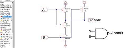
input nand gate schematic scientific diagram
Image Source : www.researchgate.net
 850 x 938 · png
nand gate layout
Image Source : mavink.com
Don't forget to bookmark Nand Gate Layout using Ctrl + D (PC) or Command + D (macos). If you are using mobile phone, you could also use menu drawer from browser. Whether it's Windows, Mac, iOs or Android, you will be able to download the images using download button.
Nand Gate Layout
Nand Gate Layout which you searching for is usable for you in this article. Here we have 29 figures about Nand Gate Layout including images, pictures, models, photos, etc. In this post, we also have variation of images available. Such as png, jpg, animated gifs, pic art, logo, black and white, transparent, etc about drone.
Not only Nand Gate Layout, you could also find another pics such as
Circuit Design,
2-Input,
Cadence,
Design,
4 Input Nand Gate Layout,
Compact,
NMOS,
Magic,
Chip,
Putty,
Diagram,
and LVS.
820 x 836 · png
cmos input nand gate students
Image Source : things-for-students.blogspot.com
1366 x 768 · png
nand gate physical layout siliconvlsi
Image Source : siliconvlsi.com
1024 x 768 · jpeg
ece lab tutorial iii hierarchical design formal verification
Image Source : www.ece.iit.edu
850 x 943 · png
diagram circuit diagram nand gate mydiagramonline
Image Source : mydiagram.online
474 x 341 · jpeg
lab laying simple circuits
Image Source : www.sccs.swarthmore.edu
0 x 0
glade tutorial input cmos nand gate layout youtube
Image Source : www.youtube.com
640 x 640 · jpeg
schematic layout input nand gates glb applied scientific
Image Source : www.researchgate.net
444 x 553 · jpeg
lab designing nand xor gates design full adders
Image Source : cmosedu.com
1276 x 655 · jpeg
lab
Image Source : cmosedu.com
0 x 0
draw input nand gate layout microwind youtube
Image Source : www.youtube.com
474 x 266 · jpeg
cmos input nand gate layout
Image Source : userfixeisenhower.z19.web.core.windows.net
412 x 687 · png
input nand gate layout
Image Source : mavink.com
0 x 0
cmos input nand gates layout diagram vlsi lec youtube
Image Source : www.youtube.com
1024 x 768 · jpeg
section digital combinational circuits powerpoint id
Image Source : www.slideserve.com
228 x 241 · jpeg
team vlsi
Image Source : www.teamvlsi.com
643 x 646 · png
virtuoso layout misidentifies connections schematic nand gate forum electronics
Image Source : www.edaboard.com
474 x 587 · jpeg
energy efficiency schools input nand gate stick diagram
Image Source : energyefficiencyschools.blogspot.com
820 x 586 · jpeg
layout design cmos input nand gate scientific diagram
Image Source : www.researchgate.net
0 x 0
cmos nand gate layout design microwind youtube
Image Source : www.youtube.com
687 x 521 · png
lab design layout simulation cmos nand gate xor gate full adder
Image Source : cmosedu.com
699 x 570 · jpeg
solved figure shows layout diagram input nand cheggcom
Image Source : www.chegg.com
930 x 1116 · png
github wateentalebschematic design simulation designing logical circuits cadence
Image Source : github.com
474 x 266 · jpeg
lecture xor gate nand gates youtube
Image Source : fity.club
474 x 540 · jpeg
digital logic nand gateuniversal gateits symbols schematics
Image Source : allabouteng.com
474 x 267 · jpeg
combinational mos logic circuits
Image Source : www.tutorialspoint.com
1274 x 603 · jpeg
transistor nand gate
Image Source : malta-miuda-e-eu.blogspot.com
474 x 184 · jpeg
xnor gate circuit diagram robhosking diagram
Image Source : robhosking.com
841 x 786 · png
input nand gate schematic scientific diagram
Image Source : www.researchgate.net
850 x 938 · png
nand gate layout
Image Source : mavink.com
Don't forget to bookmark Nand Gate Layout using Ctrl + D (PC) or Command + D (macos). If you are using mobile phone, you could also use menu drawer from browser. Whether it's Windows, Mac, iOs or Android, you will be able to download the images using download button.
Sorry, but nothing matched your search terms. Please try again with some different keywords.

